


The reference design for automotive SEPIC converters enhances modulation with a sinusoidal output of as much as 120 Hz, simplifying complicated design processes.
Discontinuous Mode (DCM) in a Single-Ended Major Inductor Converter (SEPIC) with a modulated output voltage is especially advantageous for functions in automotive and industrial programs the place effectivity, adaptability, and reliability are paramount. Using DCM permits the converter to take care of excessive effectivity throughout various masses and provide situations, enhances part longevity by lowering stress, and simplifies the management loop. Furthermore, it improves transient responses, reduces electromagnetic interference, and helps a large enter voltage vary. These advantages make DCM SEPIC converters with modulated outputs extremely efficient for steady voltage regulation in dynamic and demanding environments. Texas Devices (TI) has launched a discontinuous mode SEPIC reference design with modulated output voltage to simplify the design course of.
The automotive single-ended major inductor converter (SEPIC), using the LM5156-Q1 or LM51561-Q1 gadgets, is particularly designed to assist a modulated output voltage that includes a sinusoidal waveform of 60 VPP at as much as 120 Hz. The design encounters sure dynamic limitations when operated in several modes. When working in continuous-conduction mode (CCM), it’s dynamically restricted by the suitable half aircraft zero (RHPZ). Moreover, utilizing non-synchronous rectification at low output voltages can result in decreased discharge present on the output capacitor by the resistive load, inflicting the output voltage to not comply with the specified modulating waveform.
To handle these challenges, the magnetizing inductance is minimized to permit the facility stage to function in discontinuous mode (DCM), which successfully shifts the suitable half aircraft zero (RHPZ) past 300 kHz below the worst-case eventualities of the bottom enter voltage and most load. Nonetheless, the efficiency of the system continues to be restricted by the achieve bandwidth of the error amplifier and the Nyquist standards. With a loop bandwidth of 10 kHz, this design is able to adequately managing solely 100 Hz on the output. The DCM strategy considerably reduces Qrr ringing on the semiconductors and reduces the scale of the twin inductor.
Regardless of these enhancements, the converter generates a excessive ripple present, which in flip results in magnetizing losses, alternating present losses on the winding, and a big output ripple voltage. Nonetheless, these disadvantages are acceptable for functions requiring a most output energy of simply 18 W. One sensible utility of this know-how is in good glass modules, the place exact energy modulation and administration are essential.

Options of the design embody a loop bandwidth of 10 kHz for optimum dynamics, enabling modulation of the output voltage as much as a frequency of 120 Hz with a sinusoidal waveform. Moreover, this reference design has been absolutely constructed and rigorously examined in a laboratory setting.
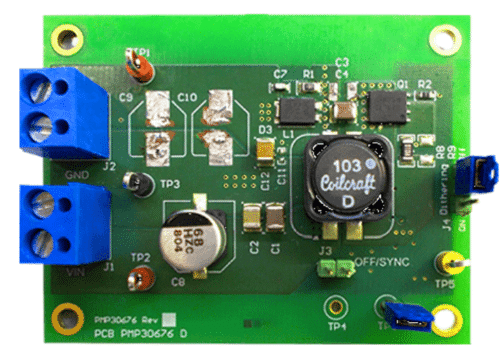
TI has examined this reference design. It comes with a invoice of supplies (BOM), schematics, meeting drawing, printed circuit board (PCB) structure, and so forth. You’ll find extra information concerning the reference design on the corporate’s web site. To learn extra about this reference design, click on right here.